Measure, model and learn to predict the lifetime of power semiconductors
디지털트윈연구실은 소재 물성부터 칩·패키지·모듈의 실측, 멀티피직스 해석, AI 예측, 수명 평가까지를 하나의 디지털 트윈으로 연결합니다. 각 단계의 결과가 다음 단계의 입력이 되고, 수명 시험 결과는 다시 모델을 보정합니다.
The Digital Twin Lab links material data, in-situ measurement of chips, packages and modules, multiphysics simulation, AI prediction and lifetime assessment into a single digital twin. Each step feeds the next, and life-test results recalibrate the model.
연구 체계: 하나로 연결된 디지털 트윈Research Framework: One Connected Digital Twin
다섯 개의 연구 축이 순환 구조로 맞물려 있습니다. 실측으로 보정한 모델이 AI를 학습시키고, AI가 빠르게 찾은 설계를 수명 모델이 검증하며, 그 결과가 다시 소재·실측 단계로 돌아옵니다.
Five research pillars interlock in a loop. Measurement-calibrated models train the AI, the lifetime model verifies the designs the AI finds, and the outcome flows back to material data and testing.
02
원자에서 시스템까지From Atoms to Systems
같은 디지털 트윈 방법론을 크기가 다른 대상에 적용합니다. 점의 색은 각 규모에서 활용하는 연구 축입니다.
The same digital-twin methodology is applied across length scales. Dot colors show which pillars are used at each scale.
ATOM · nm
원자 · 소재Atom · Material
MD로 온도·방사선 의존 물성 계산
MD for temperature- and radiation-dependent properties
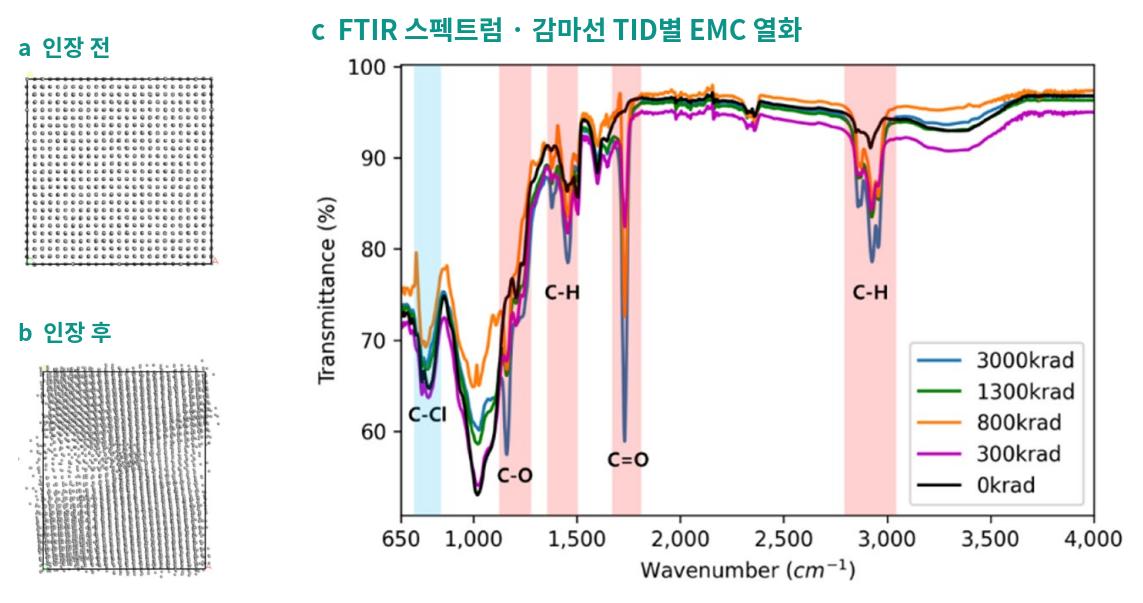
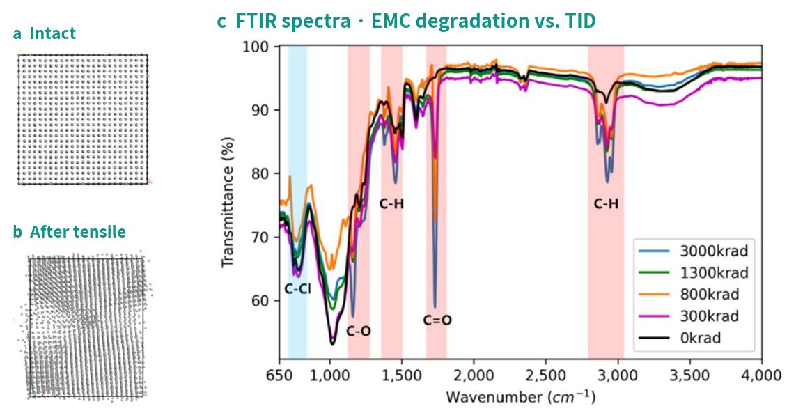
FTIR 스펙트럼과 머신러닝으로 EMC·SiN·고분자의 열·방사선 열화 정도를 판별하고, 열화에 따른 열전도도·경도 변화를 측정합니다. 문헌에 없는 물성은 분자동역학(MD) 계산으로 보완해 해석의 출발점을 바로잡습니다.
0–3000 krad감마선 TID 5단계의 EMC 열화를 FTIR 스펙트럼 + 머신러닝으로 분류
대표 연구 · EMC TID 열화 ML (JEET 2024) · SiN 방사선 열화 ML+MD (JEET 2025) · 3D 프린팅 고분자 FTIR-ANN (Appl. Sci. 2018–2020) · MD 기반 순수 Al 물성 (KSMPE 2026)
Material Property Data
“Are the inputs to our models right?”
FTIR spectra and machine learning classify thermal and radiation degradation of EMC, SiN and polymers, linked to measured changes in thermal conductivity and hardness. Molecular dynamics (MD) fills in properties the literature does not provide.
0–3000 kradfive gamma-ray TID levels of EMC degradation classified from FTIR spectra with machine learning
Key work · EMC TID degradation ML (JEET 2024) · SiN radiation degradation ML+MD (JEET 2025) · FTIR-ANN for 3D-printed polymers (Appl. Sci. 2018–2020) · MD-based pure-Al properties (KSMPE 2026)
02 · MEASURE & CALIBRATE
실측 기반 등가물성 보정
“패키지 속 칩은 실제로 어떻게 움직이는가?”
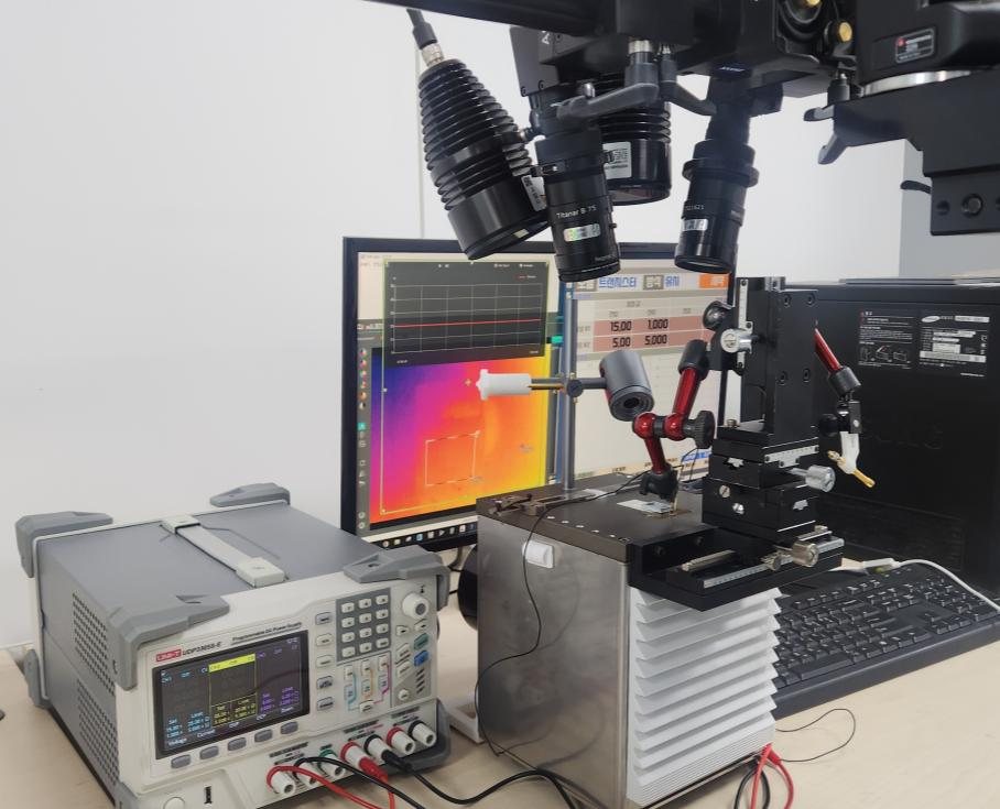
Open-top 세라믹 패키지에 칩을 실장하고 DIC·IR 열화상·I-V를 동시에 측정해, 봉지재에 가려 볼 수 없던 칩의 변형률과 온도를 비파괴로 계측합니다. 이 데이터로 칩의 등가 전기저항률·열전도도·열팽창계수를 추출합니다.
< 1 %등가물성 보정 후 전압·온도의 실측-해석 오차 (SiC 칩 15개)
대표 연구 · DIC 기반 SiC 칩 CTE 측정 (EuroSimE 2026) · Open-top 패키지 실시간 온도·변형률 동시 분석 (KSMPE 2026) · SiC PiN 다이오드 등가물성 (2025) · IGBT 8종 FEA 벤치마킹 (2025)
Measurement-based Calibration
“How does the chip really behave inside the package?”
Chips mounted in open-top ceramic packages are measured with simultaneous DIC, IR thermography and I-V sweeps, exposing strain and temperature that encapsulants normally hide. Equivalent resistivity, thermal conductivity and CTE are then extracted.
< 1 %voltage and temperature error between test and simulation after calibration (15 SiC chips)
Key work · SiC chip CTE via DIC (EuroSimE 2026) · In-situ temperature-strain analysis with open-top packages (KSMPE 2026) · Equivalent properties of SiC PiN diodes (2025) · FEA benchmarking of 8 IGBTs (2025)
03 · VIRTUAL MODEL
멀티피직스 가상 모델 · 설계 최적화
“어떤 설계 변수가 열과 응력을 지배하는가?”
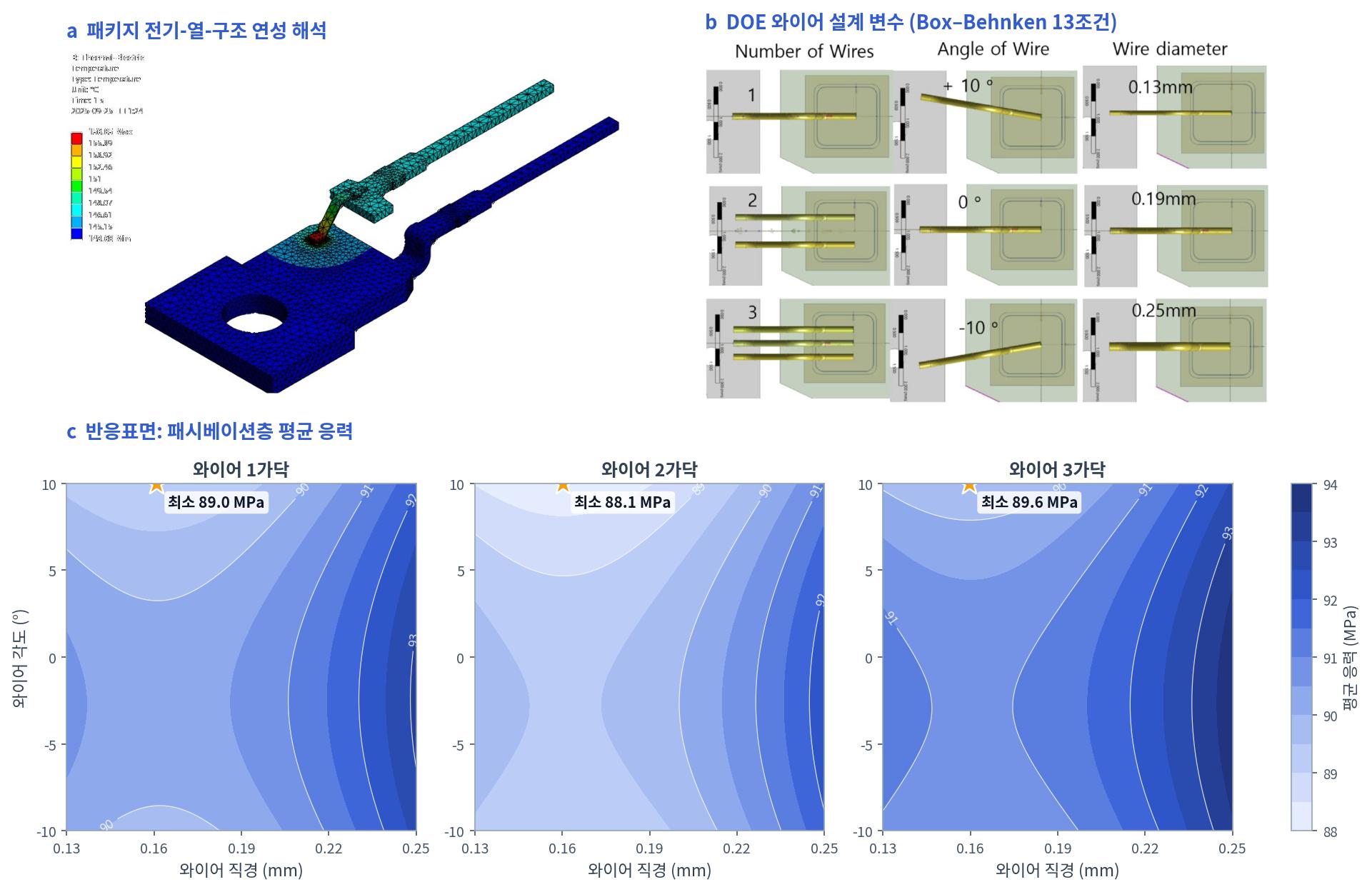
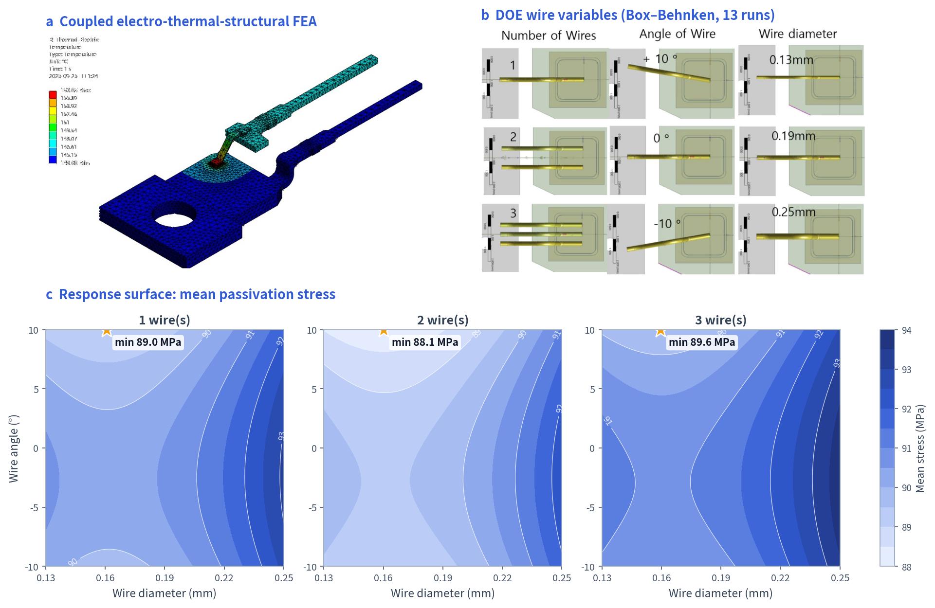
보정된 물성으로 전기-열-구조-전자기 연성 해석 모델을 만들고, 실험계획법(DOE)과 반응표면법으로 와이어·Cu 클립·솔더·메탈라이제이션·스페이서 설계를 최적화합니다. 예를 들어 SiC JBS 다이오드에서는 와이어 직경·각도·개수에 따른 칩 패시베이션층 응력을 반응표면으로 정리해 최적 본딩 조건을 제시했습니다.
100 → 0 %양면냉각 SiC 전력모듈의 다이 크랙 발생률을 구조 최적화로 제거
대표 연구 · Al 메탈라이제이션 모델링 (Energies 2025) · GaN HEMT 패키징 DOE·RSM (2025) · 양면냉각 SiC 모듈 다이 크랙 (2026) · SiC JBS 칩-패키지 상호작용 (Energy Reports 2023) · 허메틱 MOSFET 열저항 (JEET 2022)
Multiphysics Virtual Model & Design
“Which design variables drive heat and stress?”
Calibrated properties feed coupled electro-thermal-structural-electromagnetic models. Design of experiments and response surfaces then optimize wires, Cu clips, solder, metallization and spacers—for example, mapping passivation-layer stress of a SiC JBS diode against wire diameter, angle and count to find the best bonding condition.
100 → 0 %die-crack rate of a double-side-cooled SiC module eliminated by structural optimization
Key work · Al metallization modeling (Energies 2025) · GaN HEMT packaging DOE/RSM (2025) · Die cracking in DSC SiC modules (2026) · Chip-package interaction of SiC JBS diodes (Energy Reports 2023) · Thermal resistance of hermetic MOSFETs (JEET 2022)
04 · AI SURROGATE
AI 대리모델
“수천 번의 해석 없이 바로 예측할 수 있는가?”
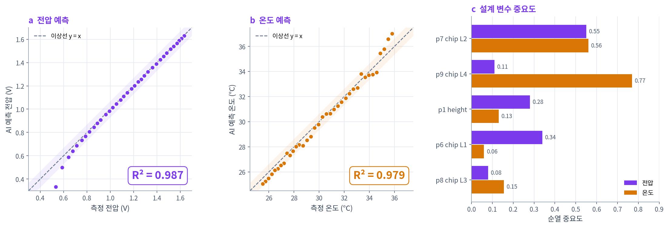
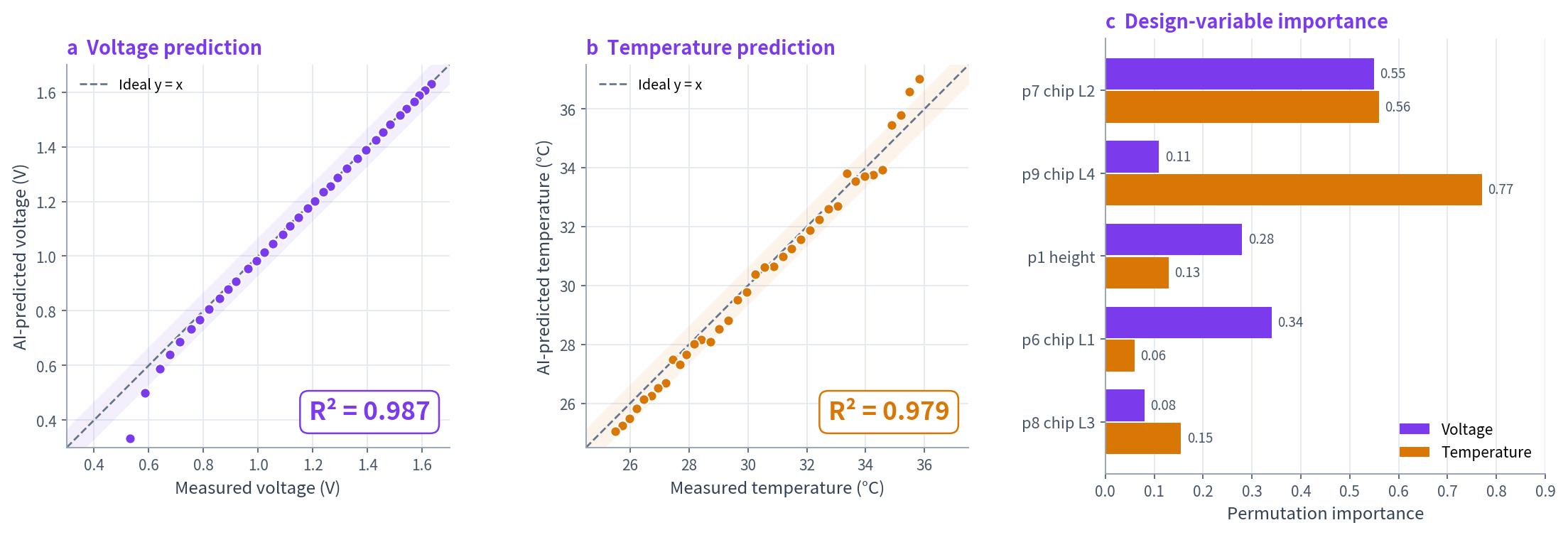
실측과 해석 데이터를 함께 학습한 물리정보 기반 머신러닝(PIML)과 앙상블 모델로, 전류·온도에 따라 변하는 칩 등가물성과 패키지 설계 응답(ΔV·ΔT)을 즉시 예측합니다.
R² ≥ 0.97IGBT 7종의 바이어스 의존 등가물성 예측 정확도
대표 연구 · Cu 클립 TO-220 전기-열 성능 PIML 예측 (KCS 2026) · IGBT 바이어스 의존 물성 예측 디지털 트윈 (KCS 2026)
AI Surrogate Models
“Can we predict without thousands of simulations?”
Physics-informed machine learning (PIML) and ensemble models, trained on both measured and simulated data, instantly predict bias-dependent chip properties and package responses (ΔV, ΔT).
R² ≥ 0.97accuracy of bias-dependent property prediction for 7 IGBTs
Key work · PIML prediction for Cu-clip TO-220 (KCS 2026) · Digital twin for bias-dependent IGBT properties (KCS 2026)
05 · RELIABILITY & LIFETIME
신뢰성 · 수명 예측
“언제, 어디서 고장 나는가?”
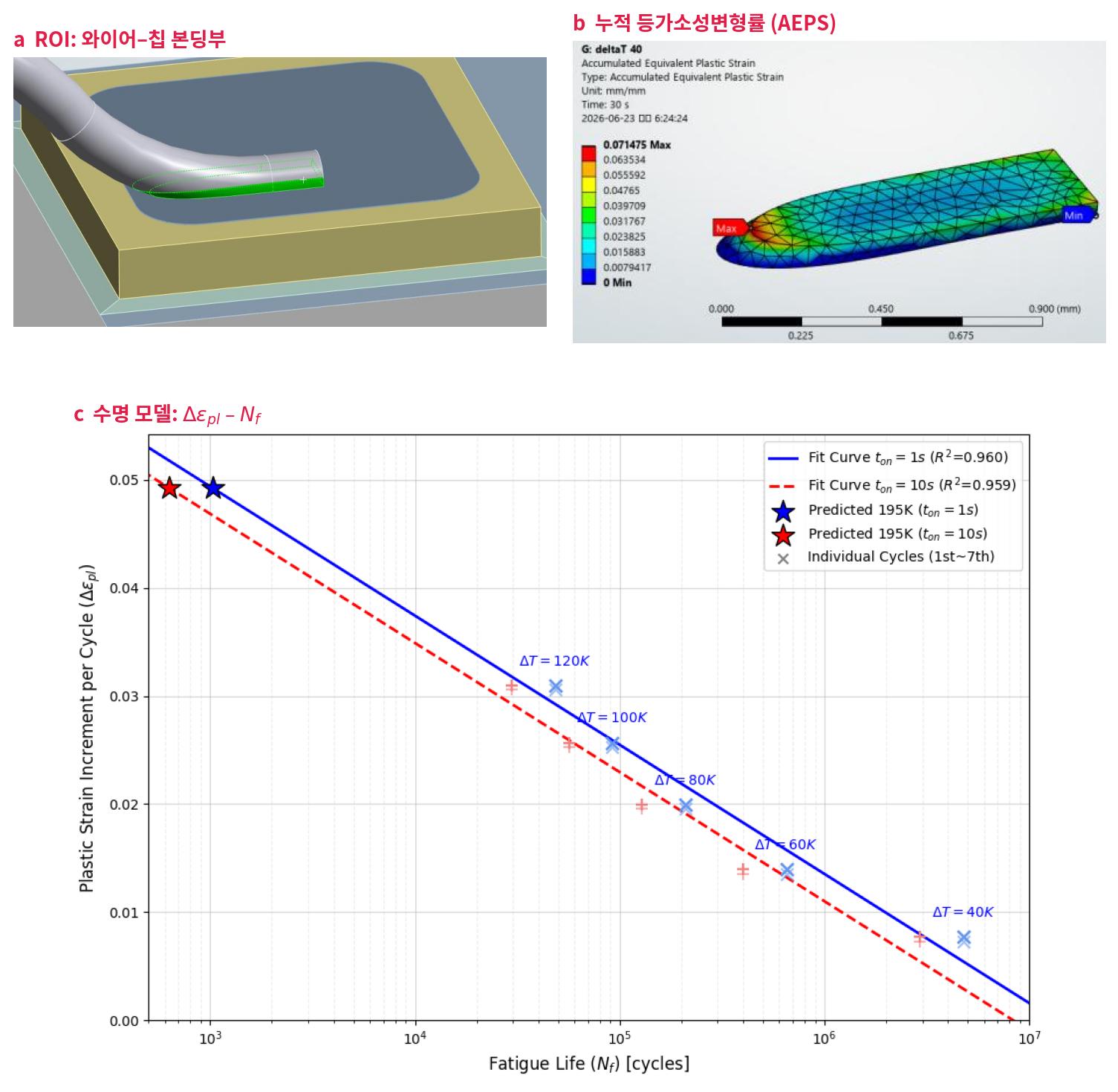
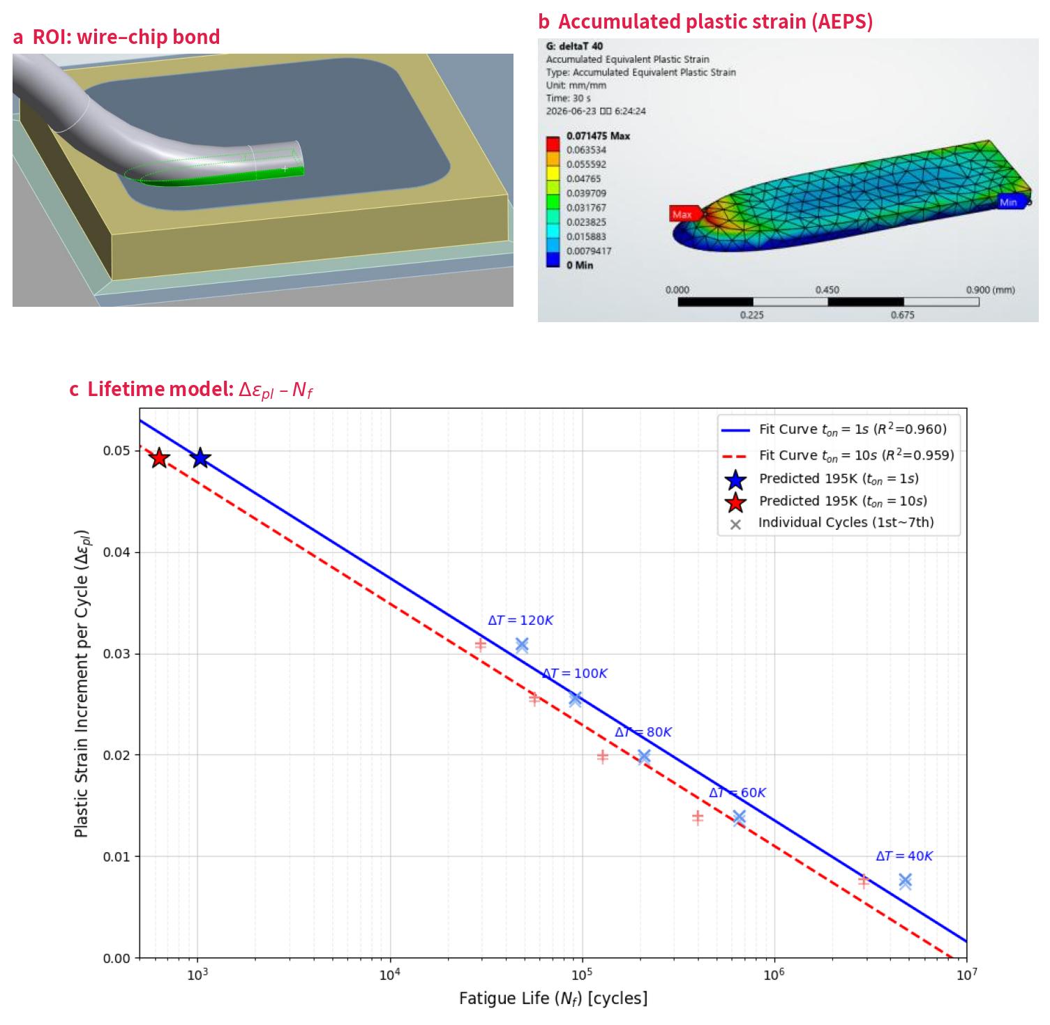
파워 사이클링을 가상으로 모사해 Al 와이어 접합 계면의 누적 등가소성변형률(AEPS)을 수명 지표로 바꾸고, 시험이 어려운 극한 온도차와 우주·원전 방사선(TID) 환경까지 수명 모델을 확장합니다.
R² = 0.96AEPS 기반 Al 와이어 수명식 피팅 정확도 (ΔT 40–195 K)
대표 연구 · AEPS 기반 Al 와이어 수명 예측 (PHM Korea 2026) · TID 효과에 따른 P-MOSFET 열화 (Microelectron. Reliab. 2025) · LED 와이어 본드 피로 수명 (Microelectron. Reliab. 2014)
Reliability & Lifetime Prediction
“When and where will it fail?”
Virtual power cycling converts the accumulated equivalent plastic strain (AEPS) at Al-wire interfaces into a lifetime metric, and the model is extended to extreme temperature swings and radiation (TID) environments that are hard to test.
R² = 0.96fit of the AEPS-based Al-wire lifetime model (ΔT 40–195 K)
Key work · AEPS-based Al-wire lifetime model (PHM Korea 2026) · TID degradation of P-MOSFETs (Microelectron. Reliab. 2025) · Wire-bond fatigue in LED packages (Microelectron. Reliab. 2014)
04
연구의 흐름How Our Research Evolved
수치해석 기법에서 출발해 LED, 3D 프린팅 소재, 전력반도체로 대상을 넓혔고, 지금은 실측과 AI를 결합한 디지털 트윈으로 이어지고 있습니다.
Starting from numerical methods, our work expanded through LEDs and 3D-printed materials to power semiconductors, and now converges into measurement- and AI-driven digital twins.